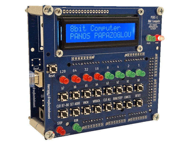
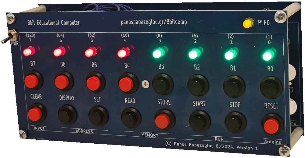
The PSOC-1 (Papazoglou Software-Oriented Computer) is an 8-bit educational computer that can be programmed in binary mode. The system is based on the Arduino MEGA 2560 platform, with the entire computer's operation handled by software within the microcontroller. The PSOC-1 features a physical user interface with LEDs and buttons.
It supports a set of assembly instructions that can be stored as 8-bit binary numbers in memory. Users interact with the system via LEDs and buttons using the binary system. For example, the instruction LOAD A, 5 is coded as 1, 5 (instruction code 1). In binary form, this instruction is represented as 0000 0001 and 0000 0101 respectively. To store the instruction in memory starting from location 10, the starting address is set as 0000 1010 (where address[10] = 1 and address[11] = 5).
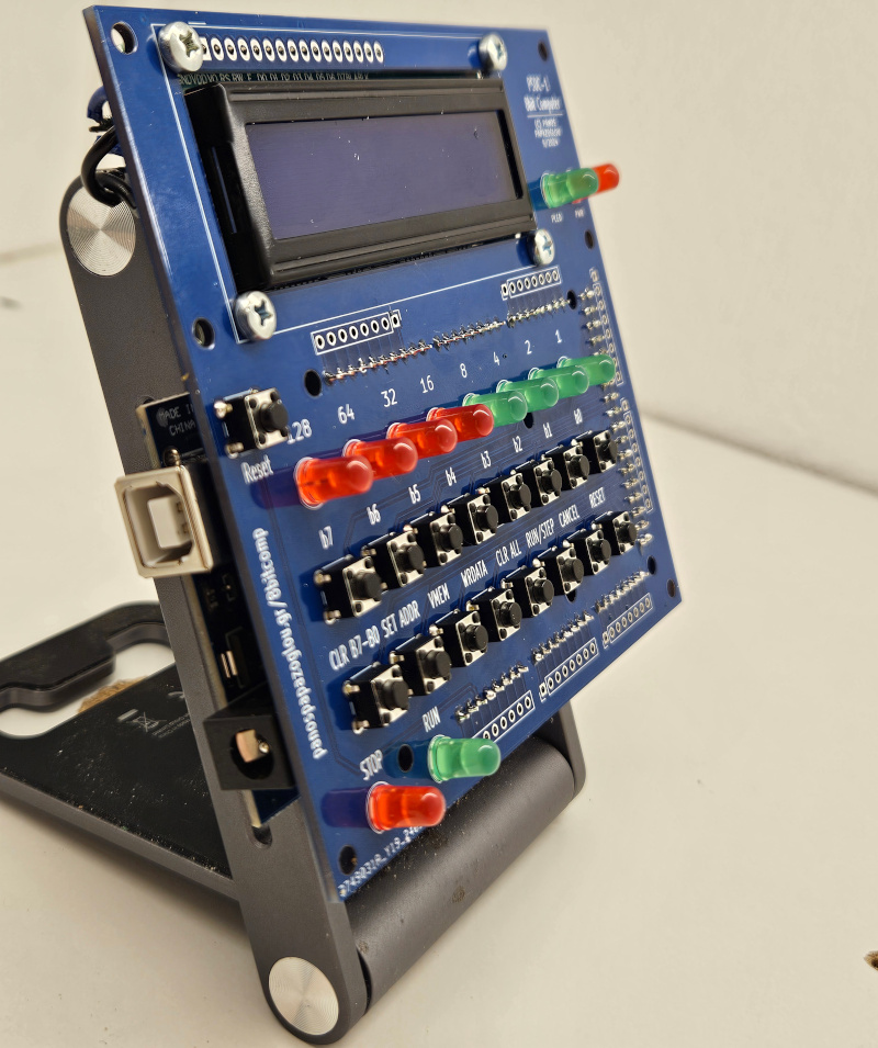
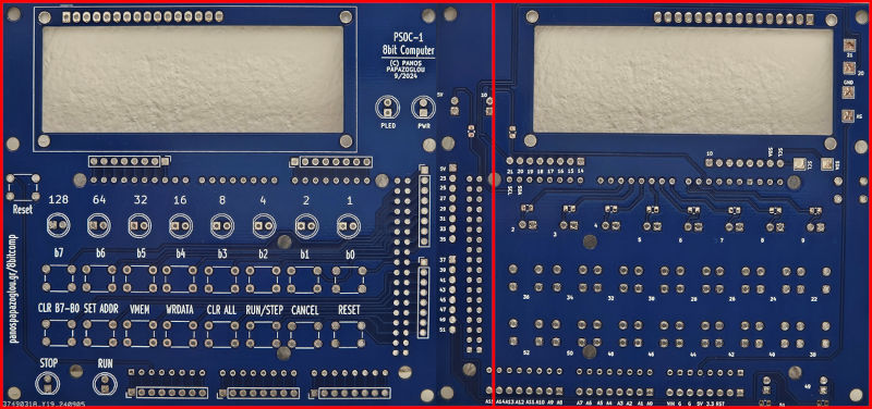
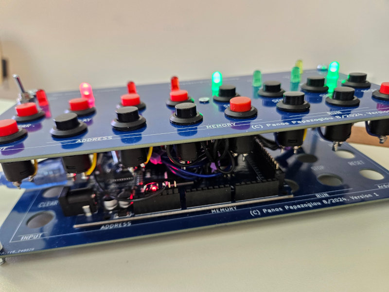
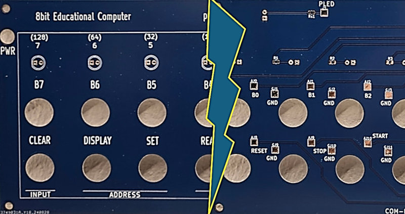
The PCB supports both the electronic circuit and the user interface (front panel).
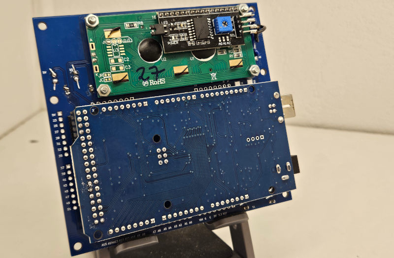
The Arduino MEGA 2560 is used to eliminate the need for external circuits to support multiple I/O pins (LEDs and buttons). A dual-purpose PCB has been designed for the front panel, supporting both LED and button operation, as well as the front panel interface. By using a PCB for the front panel, there is no need for an aluminum or 3D-printed panel.
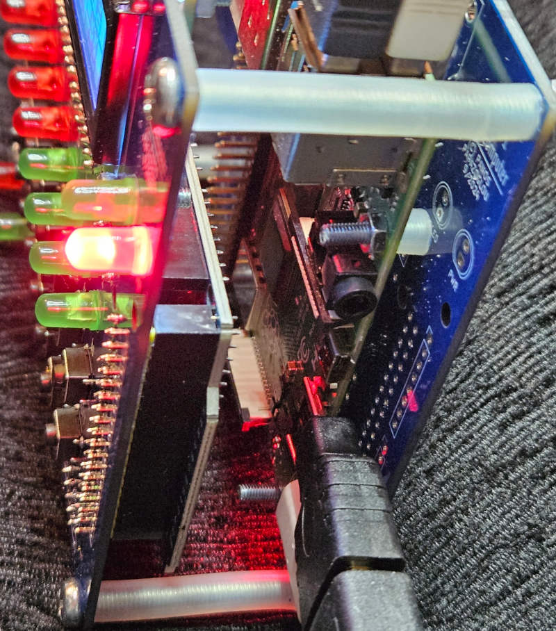
All system components are soldered onto the same board, so no cables are required. The PSOC-1 is a compact version of the prototype, which is also shown on the same page below.
To avoid using cables, the PSOC-1 PCB connects directly to the Arduino MEGA 2560 via metal pins, like a shield.
General Purpose
Accessing successive memory locations
Starting address of the next instruction to be executed
Current Address for STORE or READ content
Holds the last byte that is represented by the LEDs status
Decimal representation of the LEDs status (during input phase)
The content of OR is directly shown in the LEDs
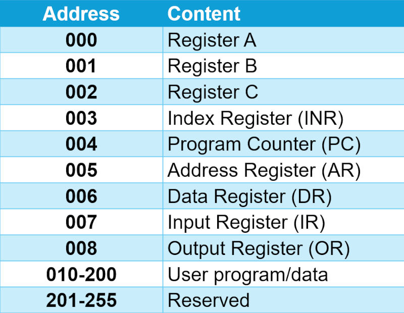
All addresses are expressed as 8-bit values, providing 256 available locations (Table 1). However, some locations are reserved for system operations. System registers are directly mapped to memory locations, making access and operation straightforward.
The memory addresses from 201 to 255 are reserved for future use, while the user can freely use the memory range from 10 to 200 for instructions and data.
Please note that some registers are not used in current version of the 8bit computer (e.g. Registers B,C,INR and DR)
The computer operation from the user’s point of view is based on a custom assembly language and the practical programming is performed through binary system. Based on this approach, the user understands how a computer works and is free to make any desired modifications.
The whole computer operation is based on software that is executed within the microcontroller of the Arduino. Thus, new assembly instructions can be developed or the existing can be modified.
In current model, only some indicative assembly instructions have been implemented.
Load an integer value (0-255) in register A
STORE [m],A (code 002)Store register A in memory location m
INC A (code 003)A=A+1
DEC A (code 004)A=A-1
JNZ m (code 5)If register A > 0, then goto address m
Every instruction reserves two bytes in memory (byte 1: instruction code, byte 2: parameter)
HALT (code 99)Program Termination
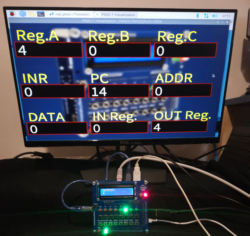
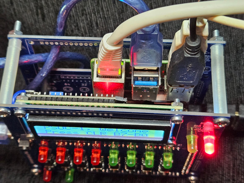
The KIT consists of three main components: the PCB panel/circuit, a 16x2 LCD display, and an Arduino MEGA 2560.
Storing the program codes at addresses [10, 11, 12, 13] and verify(for reference).
1010 [SET ADDR]
[CLR B7-B0] ; Set starting address 10
0001 [WRDATA] ; Store 1 in address 10
[CLR B7-B0]
0101 [WRDATA] ; Store 5 in address 11
CLEAR]
0010 [WRDATA] ; Store 2 in address 12
[CLR B7-B0]
1000 [WRDATA] ; Store 8 in address 13
[CLR B7-B0]
0100 [WRDATA] ; Store 4 in address 14
[CLR B7-B0]
[WRDATA] ; Store 0 in address 15
0101 [WRDATA] ; Store 5 in address 16
[CLR B7-B0]
1100 [WRDATA] ; Store 12 in address 17
[CLR B7-B0]
0110 0011 [WRDATA] ; Store 99 in address 18
[CLR B7-B0]
[WRDATA] ; Store 0 in address 19
A loop counting down from 5 to 1 will be performed step by step by pressing the [START] button successively.
It’s exciting to be inspired by the pioneers of the first personal computers, and this is part of the legacy of the vintage computer era. In 1970, John Blankenbaker designed a unique machine for its time, the first personal computer, named the Kenbak-1, which became available in 1971—earlier than any commercial microprocessor. This computer is programmed using a binary system through buttons, allowing users direct access to physical memory locations. The Kenbak-1 has no display output except for eight LEDs, which represent byte values from specific memory locations. Addresses and data are entered manually by setting the LED status using the front panel buttons.
Inspired by the general concept of the Kenbak-1, a new 8-bit educational computer (8bitCOMP) has been developed. While inspired by the Kenbak-1, the 8bitCOMP features a completely different design and implementation. Specifically, it is implemented in software within a microcontroller and features a physical user interface with LEDs and buttons.
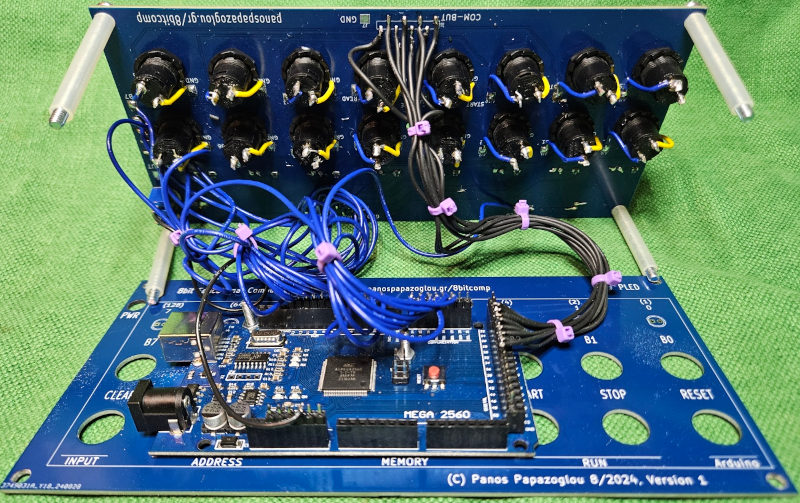
The Arduino MEGA 2560 is used to avoid the need for external circuits to support multiple I/O pins (LEDs and buttons). A dual-purpose PCB has been designed for the front panel, supporting both LED and button operation, as well as the front panel interface.
By using a PCB for the front panel, no aluminium or 3D-printed panel is required.
General Purpose
Accessing successive memory locations
Starting address of the next instruction to be executed
Current Address for STORE or READ content
Holds the last byte that is represented by the LEDs status
Decimal representation of the LEDs status (during input phase)
The content of OR is directly shown in the LEDs
All addresses are expressed as 8-bit values, providing 256 available locations (Table 1). However, some locations are reserved for system operations. System registers are directly mapped to memory locations, making access and operation straightforward.
The memory addresses from 201 to 255 are reserved for future use, while the user can freely use the memory range from 10 to 200 for instructions and data.
Please note that some registers are not used in current version of the 8bit computer (e.g. Registers B,C,INR and DR)
The computer operation from the user’s point of view is based on a custom assembly language and the practical programming is performed through binary system. Based on this approach, the user understands how a computer works and is free to make any desired modifications.
The whole computer operation is based on software that is executed within the microcontroller of the Arduino. Thus, new assembly instructions can be developed or the existing can be modified.
In current model, only some indicative assembly instructions have been implemented.
Load an integer value (0-255) in register A
STORE [m],A (code 002)Store register A in memory location m
INC A (code 003)A=A+1
DEC A (code 004)A=A-1
JNZ m (code 5)If register A > 0, then goto address m
Every instruction reserves two bytes in memory (byte 1: instruction code, byte 2: parameter)
HALT (code 99)Program Termination
In this demo, the number 3 will be stored in address 12, and the operation will be verified at the end.
Storing the program codes at addresses [10, 11, 12, 13] (for reference).
1010 [SET]
[CLEAR] ; Set starting address 10
0001 [STORE] ; Store 1 in address 10
[CLEAR]
0101 [STORE] ; Store 5 in address 11
CLEAR]
0010 [STORE] ; Store 2 in address 12
[CLEAR]
1000 [STORE] ; Store 8 in address 13
[CLEAR]
0100 [STORE] ; Store 4 in address 14
[CLEAR]
[STORE] ; Store 0 in address 15
0101 [STORE] ; Store 5 in address 16
[CLEAR]
1100 [STORE] ; Store 12 in address 17
[CLEAR]
0110 0011 [STORE] ; Store 99 in address 18
[CLEAR]
[STORE] ; Store 0 in address 19
A loop counting down from 5 to 1 will be performed step by step by pressing the [START] button successively.

Associate Professor Dr. Panayotis (Panos) Papazoglou
National and Kapodistrian University of Athens (NKUA)
Dept. of Digital Arts and Cinema
contact: papaz [at] uoa [dot] gr
Copyright © Dr. Panayotis (Panos) Papazoglou